

The Basics of Semiconductors
Semiconductors are materials with electrical properties that fall between those of conductors (like copper) and insulators (like glass). The most commonly used semiconductor material is silicon, chosen for its abundant availability and excellent semiconducting properties. Other materials such as germanium, gallium arsenide, and silicon carbide are used in specific applications where particular electronic characteristics are required.
Intrinsic and Extrinsic Semiconductors
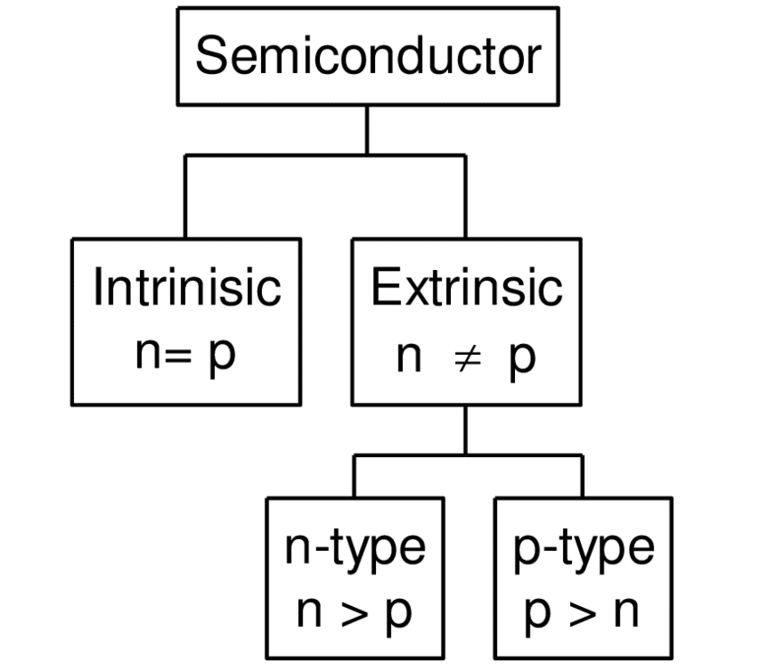
- Intrinsic Semiconductors: Pure semiconductors without any significant impurities. In their pure state, semiconductors have a very limited number of charge carriers - electrons and holes (the absence of an electron in the crystal lattice).
- Extrinsic Semiconductors: Doped with specific impurities to modify their electrical properties. There are two types of doping:
- N-type (Negative-type): Doping with elements that have more valence electrons than silicon (e.g., phosphorus). This adds extra electrons to the semiconductor.
- P-type (Positive-type): Doping with elements that have fewer valence electrons than silicon (e.g., boron). This creates "holes" or positive charge carriers.


Transistors: The Building Blocks
Transistors are the fundamental components of semiconductor chips. Acting as electronic switches, transistors can control the flow of electrical current in a circuit, which is essential for performing logical operations and data processing.
How Transistors Work
Transistors typically come in two types: Bipolar Junction Transistors (BJTs) and Field-Effect Transistors (FETs).
1. Bipolar Junction Transistors (BJTs): These transistors have three layers of semiconductor material, forming two p-n junctions. They come in two varieties:
- NPN Transistors: A layer of p-type material sandwiched between two n-type layers.
- PNP Transistors: A layer of n-type material sandwiched between two p-type layers.
In a BJT, a small current injected into the base region controls a larger current flowing between the collector and emitter.

2. Field-Effect Transistors (FETs): These are controlled by voltage rather than current. The most common type is the Metal-Oxide-Semiconductor FET (MOSFET), which has four terminals: source, drain, gate, and body. The voltage applied to the gate terminal controls the current flow between the source and drain.

Integrated Circuits: Combining Transistors
An integrated circuit (IC) combines millions or even billions of transistors into a single chip to perform complex functions. The ICs are designed to handle specific tasks such as processing data (central processing units or CPUs), storing data (memory chips), or managing power (power management ICs).
Logic Gates and Circuits
At the heart of ICs are logic gates, which perform basic logical functions based on Boolean algebra. These include:
- AND Gate: Outputs true only if all inputs are true.
- OR Gate: Outputs true if at least one input is true.
- NOT Gate: Inverts the input signal (true becomes false, and vice versa).
- NAND Gate: Outputs false only if all inputs are true.
- NOR Gate: Outputs true only if all inputs are false.
- XOR Gate: Outputs true if inputs are different.
Combining these gates in various configurations allows the creation of more complex circuits capable of performing arithmetic operations, data storage, and data manipulation.
The Manufacturing Process of Semiconductor Chips
The creation of semiconductor chips involves several sophisticated steps, each requiring precision and advanced technology.
1. Design
The process begins with designing the chip. Engineers use specialized software tools (Electronic Design Automation or EDA tools) to create a blueprint of the chip's architecture. This design includes the layout of transistors, interconnections, and other components.
2. Wafer Production
Once the design is complete, the manufacturing process starts with the production of silicon wafers. A pure silicon crystal is grown using the Czochralski process, where a seed crystal is dipped into molten silicon and slowly pulled out while rotating. This creates a large single crystal of silicon, which is then sliced into thin wafers.
3. Photolithography
Photolithography is a key step in defining the intricate patterns of the chip. The process involves several stages:
- Coating: The silicon wafer is coated with a light-sensitive material called photoresist.
- Exposure: A mask containing the pattern of the circuit is placed over the wafer. Ultraviolet light shines through the mask, transferring the pattern onto the photoresist.
- Developing: The wafer is developed, removing the exposed (or unexposed, depending on the type of photoresist) areas of the photoresist, leaving the pattern on the wafer.
4. Etching
Etching removes the unprotected silicon areas, carving out the intricate patterns. This can be done using chemical (wet etching) or plasma (dry etching) techniques.
5. Doping
To modify the electrical properties of the silicon, specific impurities are introduced through a process called doping. This is typically done using ion implantation, where ions are accelerated and embedded into the silicon substrate.
6. Layering and Interconnection
Modern chips require multiple layers to create complex circuits. Layers of various materials, such as silicon dioxide (an insulator) and metals (conductors), are deposited on the wafer. Each layer is patterned and etched to create interconnections between transistors and other components.
7. Planarization
Planarization ensures that each layer is flat and smooth, essential for the accuracy of subsequent layers. This is typically achieved through Chemical Mechanical Polishing (CMP).
8. Testing and Packaging
After the wafer processing is complete, the individual chips are tested for functionality. Functional chips are cut from the wafer, packaged in protective casings, and tested again before being shipped to customers.
Advanced Features and Technologies
As semiconductor technology advances, new features and technologies are integrated into chips to enhance their performance and capabilities.
Multi-Core Processors
Modern CPUs often contain multiple cores, each capable of executing instructions independently. Multi-core processors improve performance by allowing parallel processing, where different tasks are handled simultaneously by different cores.
System on Chip (SoC)
An SoC integrates all necessary components of a computer or other electronic system onto a single chip. This includes the CPU, memory, input/output ports, and more. SoCs are commonly used in smartphones and other compact devices, offering high performance in a small footprint.
FinFET and 3D Transistors
To continue the trend of miniaturization and performance improvement, new transistor designs such as FinFET (Fin Field-Effect Transistor) have been developed. FinFETs have a 3D structure that allows better control over the electrical current, reducing leakage and improving efficiency.
The Role of Software in Chip Functionality
While the hardware provides the physical foundation, software is essential for making chips functional. The design and manufacturing processes are guided by sophisticated software tools that simulate and validate the performance of the chip before production.
Firmware and Microcode
Firmware is low-level software embedded in hardware devices, providing the necessary instructions for the hardware to communicate with other devices and the operating system. Microcode is a layer of hardware-level instructions that control the processor’s operations, allowing it to execute complex machine instructions.
Conclusion
Understanding how semiconductor chips work reveals the incredible complexity and ingenuity behind these tiny devices. From the fundamental properties of semiconductors and the basic workings of transistors to the sophisticated manufacturing processes and advanced technologies, every aspect of chip design and production involves cutting-edge science and engineering. As we continue to push the boundaries of what semiconductor chips can do, they will undoubtedly remain at the heart of technological innovation, driving advancements across countless fields and industries.
